What is Top-Down Nanofabrication?
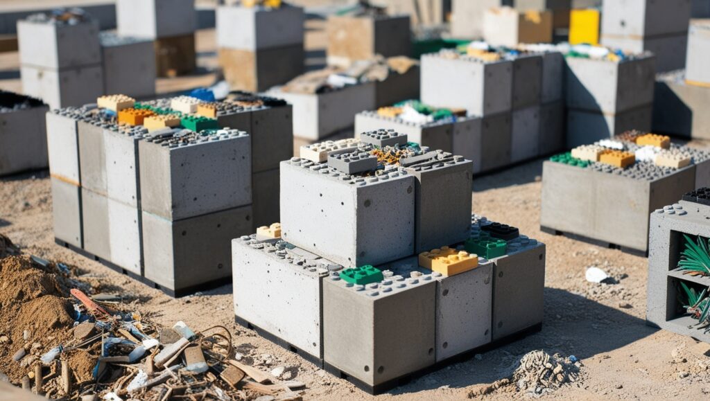
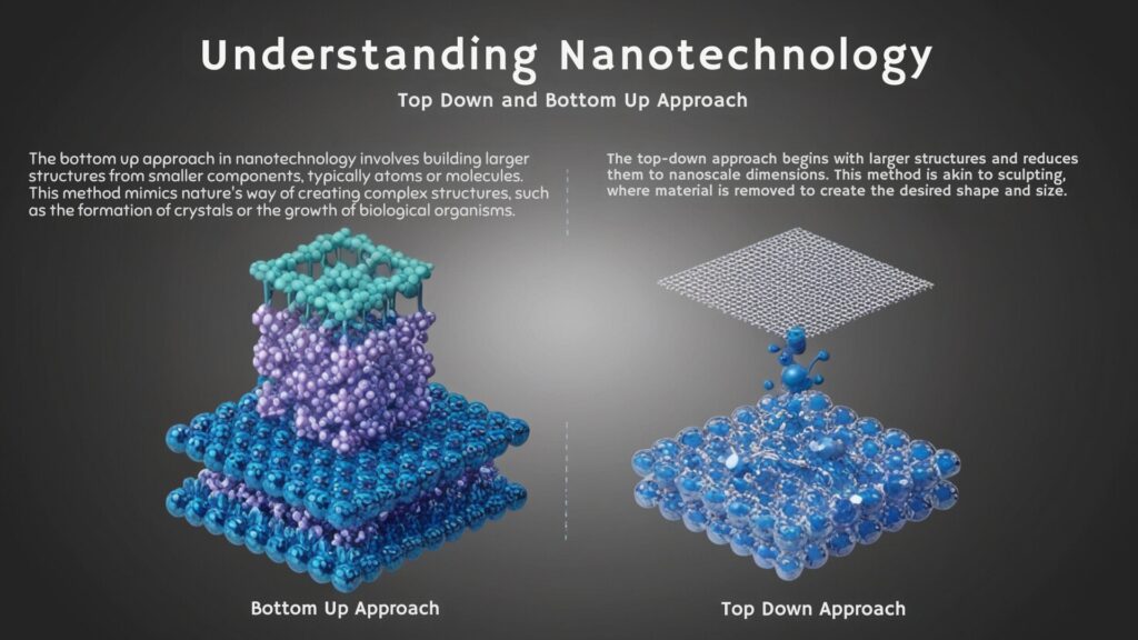
Top-down nanofabrication is a method in which bulk materials are progressively reduced to create nanoscale structures. This approach can be likened to a sculptor carving out a statue from a template by removing material, rather than building up from the atomic level. One of the most significant techniques within this method is photolithography, where short wavelength light or electrons (in the case of e-beam lithography) are used to pattern a photoresist. Subsequent etching processes, such as chemical, plasma, or reactive ion etching, then remove the material beneath the photoresist to form the desired nanostructure.
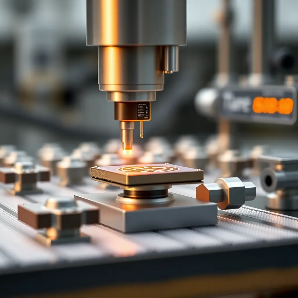
Etching plays a crucial role in top-down nanofabrication. This process involves removing material from a surface through chemical or physical means, with reactive ion etching (RIE) and deep reactive ion etching (DRIE) being particularly prevalent in nanoscale applications.
Top-down approaches are advantageous for creating structures with long-range order and facilitating macroscopic connections, making them suitable for various industrial applications, including the semiconductor industry, which leverages these methods to enhance the performance of products like smartphones. The combination of top-down and bottom-up techniques is anticipated to offer the most comprehensive set of tools for advanced nanofabrication, marrying the benefits of both strategies.
Techniques
Several methods are employed in top-down nanofabrication, each with distinct advantages and applications.
- Lithography: Various lithographic techniques, such as optical lithography, electron beam lithography, and nanoimprint lithography, are crucial in defining nanoscale patterns on substrates. These techniques allow for precise control over the dimensions and arrangements of the structures being fabricated.
- Etching: This process involves selectively removing layers from the surface of a material, using chemical or physical means to create the desired nanostructures. Both wet and dry etching techniques are utilized, with dry etching offering higher resolution.
- Deposition: Physical vapor deposition (PVD) and chemical vapor deposition (CVD) techniques are often used in conjunction with lithography to add material layers onto the substrate, allowing for complex device architectures to be built up layer by layer.
Examples of Top-Down approach in nanofabrication
| Technique | Description | Advantages | Disadvantages |
| Ball Milling | High-energy impacts break down bulk materials into nanoparticles. | Simple and scalable | Limited size control, potential damage to material properties |
| Photolithography | Uses light to create patterns on a material, followed by etching to form desired structures. | High resolution, established technology | Expensive, limited to specific materials, complex process |
| Electron Beam Lithography | Uses an electron beam to create high-resolution patterns on a material. | High resolution, versatile for various materials | Expensive, slow process |
Advantages of the Top-Down Approach:
- Established and reliable: Top-down techniques have been around for a while, making them well-understood and reliable for specific applications.
- Precise control over features: In certain cases, this approach offers precise control over the size and shape of the fabricated nanostructures.
Disadvantages of the Top-Down Approach:
- Not all materials are created equal: Some materials don’t react well to the intense forces involved in top-down processes, potentially compromising their integrity.
- Waste not, want not (except sometimes): The process often generates significant waste material, raising environmental concerns.
What is Bottom-Up Nanofabrication?
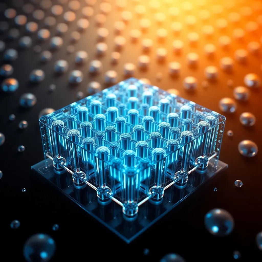
Bottom-up nanofabrication is a method of creating nanoscale materials and devices by assembling them from smaller units like atoms or molecules. This approach leverages self-assembly and templating techniques to build structures layer by layer, often mimicking natural processes. By focusing on the assembly of these small components, bottom-up methods can achieve higher precision and potentially lower costs in producing nanostructures compared to traditional top-down approaches. Additionally, bottom-up nanofabrication is often more environmentally friendly since it minimizes waste by using only the necessary materials.
Self-assembly in bottom-up nanofabrication can lead to complex structures that are difficult to achieve with conventional fabrication techniques, allowing for innovative designs in nanotechnology. This method also has a better chance of producing nanostructures with fewer defects, a more homogenous chemical composition, and better short- and long-range ordering compared to the top-down method.
Examples of Bottom-Up Techniques in Nanofabrication
| Technique | Description | Advantages | Disadvantages |
| Chemical Vapor Deposition (CVD) | Precursor chemicals react to form a solid film on a substrate, allowing for precise control over thickness and composition. | Versatile, high purity materials | Complex equipment, can be expensive |
| Sol-Gel Synthesis | Liquid precursors undergo chemical reactions to form a gel, which is then converted into a solid nanomaterial. | Simple, low-cost, diverse materials | Limited control over size and shape |
| Self-Assembly | Materials spontaneously organize into desired structures due to their inherent properties. | Can create complex structures, minimal waste | Unpredictable, limited control over process |
Advantages of the Bottom-Up Approach:
- Atomic-level control: Bottom-up methods potentially offer greater control over the atomic-level structure of the material, leading to unique properties.
- Eco-friendly nanofabrication: This approach inherently minimizes waste generation, making it a more environmentally friendly option.
Disadvantages of the Bottom-Up Approach:
- Scaling up the fun: Scaling up bottom-up production to meet industrial demands can be challenging and requires further development.
- Controlling the microscopic orchestra: Precisely controlling the assembly process at the atomic level can be complex and requires specialized expertise.
Comparison of Top-Down and Bottom-Up Approaches
The comparison between top-down and bottom-up approaches in nanofabrication highlights distinct methodologies, advantages, and challenges associated with each technique.
Overview of Approaches
The top-down approach begins with larger structures, progressively etching or carving them down to nanoscale dimensions. Techniques such as photolithography and etching are commonly employed, allowing for the creation of nanoscale structures with high precision and control, essential for applications like semiconductor manufacturing. In contrast, the bottom-up approach constructs materials atom by atom or molecule by molecule, facilitating greater precision and the ability to design complex nanoscale architectures through methods like self-assembly.
Advantages and Limitations
Precision and Control
Both approaches excel in precision, but their methodologies differ. The top-down approach is effective in creating intricate patterns with sub-nanometer resolution, beneficial for well-defined structures. However, it may face challenges in achieving atomic-level precision and uniformity across larger areas, as it operates primarily on a two-dimensional plane. On the other hand, the bottom-up approach allows for manipulation at the atomic level, enabling the design of materials with specific properties, but may require more specialized equipment and expertise, leading to higher costs and complexity.
Scalability
Scalability is another critical factor. The bottom-up approach is highly scalable; chemical synthesis techniques can easily be scaled up to produce nanomaterials in bulk, making it suitable for mass production applications. Conversely, the top-down approach can struggle with scalability due to the challenges of maintaining uniformity and reproducibility when modifying bulk materials.
Cost and Accessibility
From a cost perspective, the top-down approach has the advantage of utilizing well-established methodologies that have been optimized over decades. This accessibility can lead to cost-effective solutions in industries that have existing fabrication processes. In contrast, the bottom-up approach may involve more complex processes and specialized equipment, potentially increasing overall implementation costs.
Factors Influencing Choice of Nanofabrication Methods
Several factors influence the choice between top-down and bottom-up approaches in nanofabrication, each offering distinct advantages and challenges that impact their suitability for different applications.
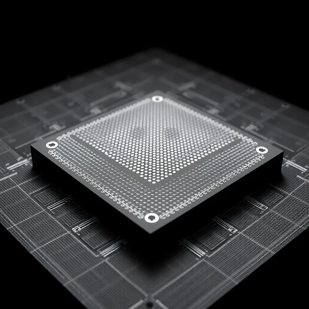
Firstly, the scale and complexity of the desired nanostructures play a crucial role. Top-down methods such as lithography are typically preferred for creating intricate and precise patterns over larger areas, making them ideal for applications like integrated circuits and microelectromechanical systems (MEMS). These methods allow for high precision and control, essential for the uniformity and alignment required in electronic components.
In contrast, bottom-up approaches are more suited for synthesizing nanoscale materials with unique properties that emerge at the atomic or molecular level. Techniques such as chemical vapor deposition (CVD) and molecular self-assembly (MSA) are advantageous for their ability to produce materials with high purity and crystalline quality. These methods are particularly effective for creating nanomaterials such as carbon nanotubes, quantum dots, and nanowires, where the properties of the material are inherently dependent on their nanoscale dimensions.
Cost and scalability also significantly influence the decision. Top-down approaches can be cost-prohibitive due to the expensive equipment and materials required for processes like electron beam lithography and focused ion beam lithography. On the other hand, bottom-up methods can be more cost-effective and scalable, particularly for bulk production of nanomaterials, as they often involve simpler chemical processes and equipment.
The intended application further guides the choice. For example, in biotechnology, where the integration of biological molecules with nanostructures is crucial, bottom-up methods such as molecular self-assembly are favored for their ability to create biocompatible and functional nanostructures. Meanwhile, in semiconductor manufacturing, the high resolution and repeatability of top-down methods are essential to meet the stringent requirements of the industry.
Ultimately, the optimal balance between top-down and bottom-up approaches is determined by a combination of these factors, requiring careful consideration of the specific requirements of the nanofabrication project at hand.
